
16 Bit I2C ADS1115 Module ADC 4 channel with Pro Gain Amplifier RPi (WHL #26)
Meep. We finally have a new product review, after all that editorial, recap and electronic load rubbish ![]()
Today’s item in the mail is an I²C ADC on a small PCB, running four channels (or two differential ones) with 16 bit precision. Sounds nice? Well, if it holds the claimed specs, it IS a nice product! I bought it in mid-June on AliExpress for 2.06 USD. Adafruit, by the way, charges 15 bucks for the exact same thing. Do I smell profit margin?
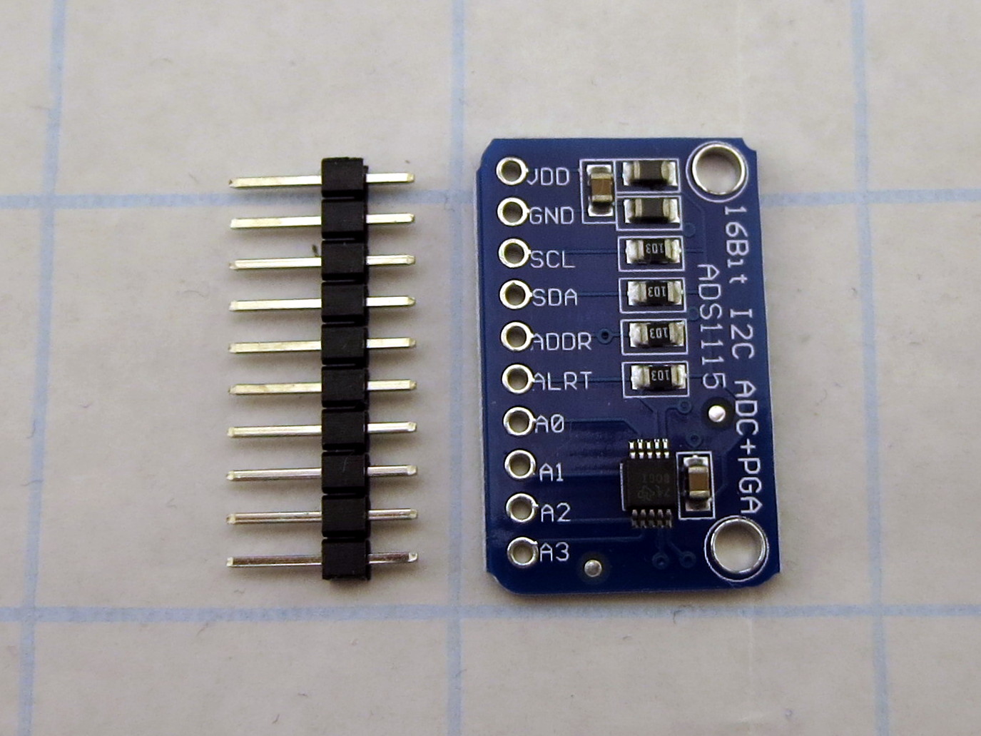
Here’s how it looks straight out of the ESD bag:
Backside is a tad boring (keep the VDD in mind):
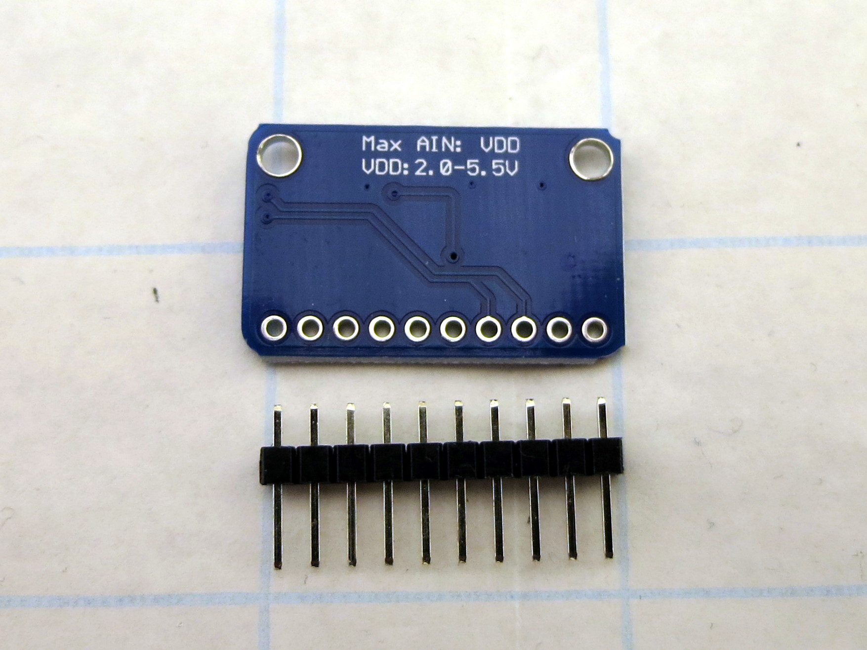
(there’s a floating island on the GND plane, boo!)
So, what does the friendly Asian seller claim?
ADC Bit rate: 16 Bit
Interface Type: I2C
Channels: 4 Channel AN0 AN1 AN2 AN3 or 2 differential inputs
Input voltage: 2.0-5.5v
Channel input voltage :0-VDD
Continuous Mode: Only 150μA
Single-Shot Mode: Auto Shut-Down
PROGRAMMABLE DATA RATE:8sps-860sps
Input range programmed control, 7 types input ranges:
-0.256V ~ + 0.256V, -0.512V ~ + 0.512V, -1.024V ~ + 1.024V,
-2.048V ~ + 2.048V, -4.096V ~ + 4.096 V, -6.144V ~ + 6.144V
I2C 7-bit addresses between 0x48-0x4B
Size:18mm*28mm
Which is, apart from the board size, basically straight from the datasheet of the ADS111x family of ADCs. The ADS1114 and ADS1113 are just ADCs with fewer channels, the ADS1115 is top of the line in this family.
Assembly is as easy as it gets:
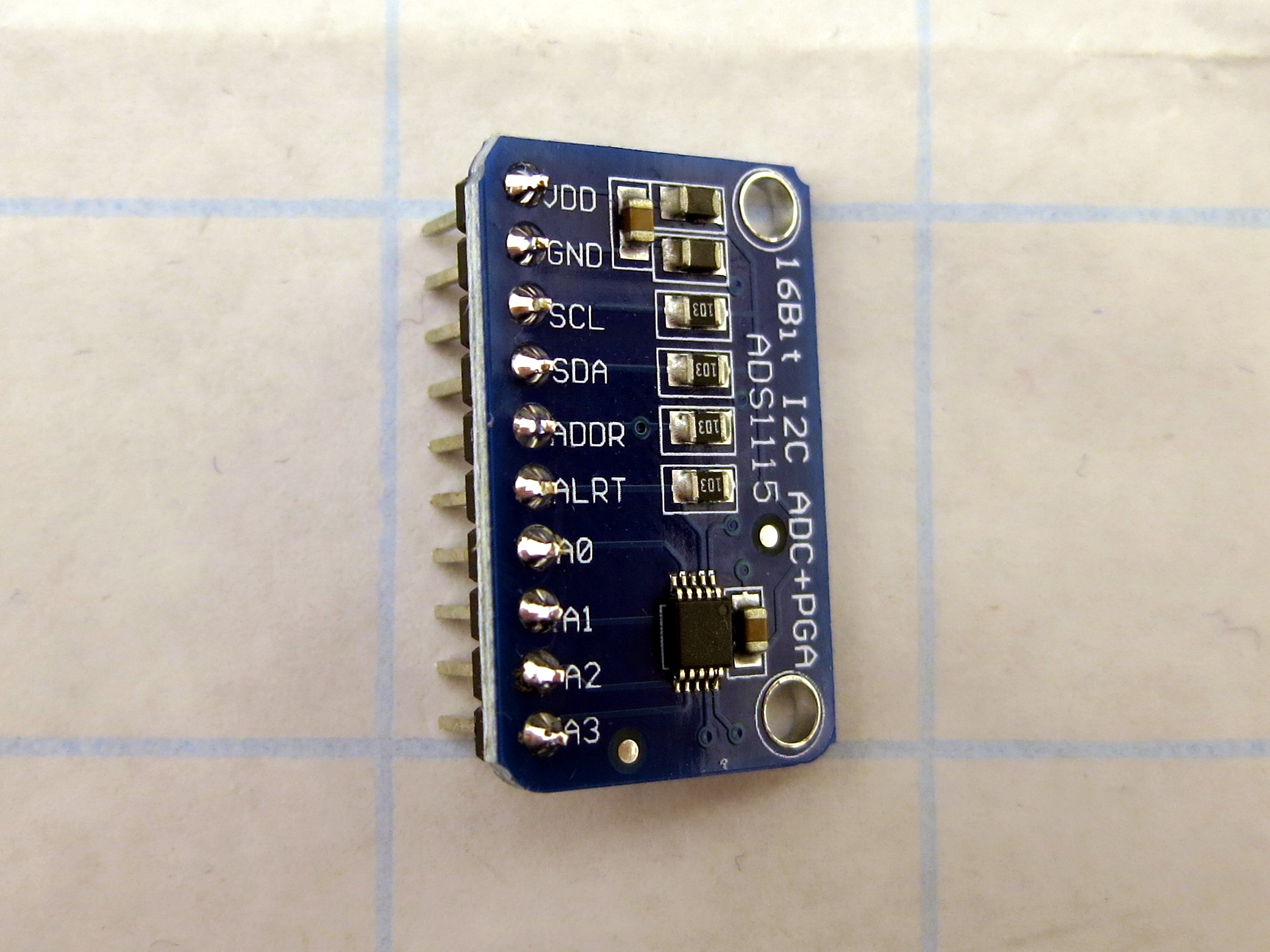
(Decent but not perfect; I hope it will make up for the horrors of the flux massacre in some recent post ![]() )
)
The board actually uses the larger package type of the ADC, as there is the VSSOP option with HUGE 3.0×3.0mm² package size and 0.5mm pin pitch, and there’s a X2QFN option with 2.0×1.5mm² with same pin pitch, but there are some horizontal and some vertical pin strips to make them fit in that footprint. Choose your poison.
The address pin (#1) is wired to GND per 1k resistance, which will make the chip select 1001000 = 0x48 as I²C address. Upon further inspection, I guess removing this resistor will make the ADDR pin on the header usable. The chip has the ability to also use address 1001001 = 0x49 when connected to VDD, as well as 1001010 = 0x4A on SDA and 1001011 = 0x4B on SCL. If nothing else connects to your microcontroller, 0x48 should be absolutely fine.
Now, the chip itself has the TI logo on it, but only says “74” and “BOGI”. Probably bogius, but the Adafruit product image doesn’t show much difference, so I assume that is correct…still, Mouser for example charges you well over 2€ for it. When buying entire reels of 2500pcs… ![]()
How to interface it with an Arduino? Well, search for your SDA/SCL pins and hook them up, supply VDD/GND (from the regulated 5V/3.3V on the Arduino board is fine). There’s a great library on github where Adafruit offers a config file for both ADS11xx as well as ADS10xx chips (the latter have 12 bit ADCs) and a minimalistic example. Add that to your library path and you’re good. It takes care of the different settings, e.g. single-ended vs. differential measurements, gain settings = range selection, and more. Just don’t run your inputs above 5.5V, even if you’ve got max VDD and got the ±6.144V range selected!
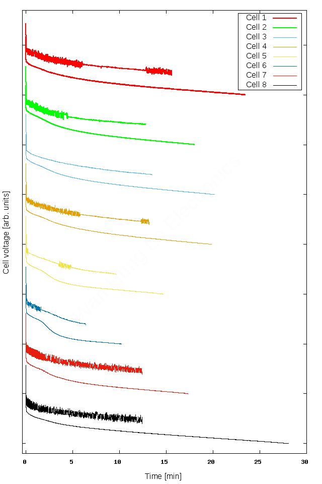
I know I shouldn’t waffle on and present some facts to you…so, after sadly removing one of the promised 16 bits as sign bit (for differential measurements), we’re left with 32768 steps in the chosen voltage range. That’s still plenty to upgrade our old graph from the Arduino ADC with the weird, trembling readings…

…to this puppy:

Nice, isn’t it? ![]()
You’ll probably notice that the x-axis has changed significantly, although discharge current was about the same at 2 amps. That’s not only due to better (more precise) readings of the cutoff voltage, but also because of some slightly changed wiring. You know, there’s a reason for 4-wire measurements, and doing so when discharging batteries to some exact cutoff voltage really helps squeezing out a bit more. I mean, the voltage drop of my Hirschmann measuring leads is startling, these are said to be 16A types and they are only one meter each in length – but having large test setups across your desk always requires some performance sacrifices. So now there’s another two wires to directly tap off the voltage very close to the battery….
Moreover, there’s a pronounced kink visible for cell 6, and to lesser extent, for cell 5. That’s not the typical discharge curve, this has to have something to do with the ageing of the cell. As other cells do not show such behaviour, it’s highly unlikely that my test setup is the root cause for it. So the internal resistance goes up at some point above 3.4 volts…I initially thought about a thermal effect, as the batteries do get warm in the process. At the end of the discharge, all of them were around 35 to 37°C, compared to room temperature of 24°C. Thing is: Heating up a cell should lower the internal resistance, as chemistry almost always works better with elevated temperatures – hence the “+10K = double the rate of reaction” rule. So even if the cells do get hot around this 3.4V point, it cannot explain the sudden drop in internal resistance and therefore voltage.
Here’s the full graph with old and new measurements, the new ADS1115 measurements are downshifted slightly so that the traces aren’t overlapping that much:
Again, the runtime difference is mostly because of the more precise voltage measurement and therefore later cutoff. As this is a constant current mode test (2 amps), changing axis from time to (m)Ah is just a matter of the correct conversion factor. You can do the maths yourself, but be assured these cells are nowhere fresh and deliver less than 50% of their capacity at that relatively high current. I couldn’t be bothered yet to run at let’s say 0.1C, that’ll need some more lines of C code to not use the computer as a logging device.
Testing another brand of cells, a Panasonic CGR18650 type – mostly empty and also quite aged:

Where’s the green trace coming from? ![]()
Guess what, when using a voltage divider for the main voltage measurement (~1:19 in current test setup), the voltage ranges can be set much lower. As long as there is some current flowing to the ADC (RTFM) and it’s not down in regions where you are affected by shot noise from your resistors, there should be no downsides in doing so. As this setting affects all of the ADC inputs, the second channel is much more sensitive – and 15 bits are plenty to pull off a neat, yet not recommended, little trick: Remember the MOSFET that acts as a switch for cutting off the voltage once the battery is discharged? The little IRFP4668 beasty carries all current and has a RDSon of 10mΩ. Electrons that grunt through a resistor will lose some energy…and measuring that voltage drop across the 10mΩ of RDSon is absolutely within reach. No separate shunt resistor required*! (*for crude measurements, that is)
Also, you can see the setting of the Arduino program that allows for resuming the current once the cutoff voltage was detected. One could empty the battery bit by bit, squeezing out every little drop of current. Of course, I’d re-adjust the current once the individual steps are shorter than a few dozen seconds, but in principle you can use this to totally deplete the battery. Electrochemistry is a strong but predictable opponent…
What else have we got? Some stability measurements, with the Statron lab supply as source. A tad long and messy, but doing 30 measurements with up to 2k data points wasn’t easy either ![]()

This is the combined noise level of lab power supply, the electronic load at around 3/4 amps, the ADC and some looong wires. Sure, there are some spiky moments, but overall the noise level is pretty decent. The calculated standard deviation of these individual tests were below 7mV in all cases, and that’s more than good enough for me. Especially the 3-4-5V ones (lithium batteries!) are smooth, which might be due to a good choice in regard to the transformer tabs of the device. There’s also no huge changes in noise level when the ADC switches ranges, e.g. from 19V to 20V in this test. When displaying the 1V voltage difference between every trace to scale, you wouldn’t see a thing. Or, you wouldn’t fit two traces onto one screen ![]() (total y range is 1.25V, traces are offset in a linear fashion according to their average values)
(total y range is 1.25V, traces are offset in a linear fashion according to their average values)
Also, drift doesn’t appear to be an issue at all. Again, some traces wander around more than others (oscillations at 7V for example!), but overall none of the devices drifts over time. That’s excellent!
One more thing: I know it is not made for this, but without the load MOSFET kicking in, the current draw should be minimal. What about absolute accuracy and linearity of the readings ?

In here, I’ve measured my quad voltage reference that hasn’t gotten a review yet. It’s made from the good old AD584“LH” (that isn’t listed in AD’s datasheets, go figure…) and back when I did project #P1, I verified the hand-written voltage readings with a calibrated Keithley 2700 DMM. They were spot-on, and so I trust the device up to a few tenths of a millivolt…let’s say one millivolt if you ignore temperature drift completely.
The traces are obviously offset once again to zoom in deep enough to see the ADC noise. The y tics are actually 10mV apart and the straight lines indicate the 2.49888V, 5.00170V, 7.50005V and 10.00238V reference voltages. So linearity is a slight issue – the lower values read a tad low, while the higher ones overshoot slightly.
Precise values are:
(2495.47±1.46)mV -> 4.41mV / 0.14% low
(4999.37±2.40)mV -> 2.33mV / 0.05% low
(7502.90±1.42)mV -> 2.85mV / 0.04% high
(10008.63±1.15)mV -> 6.25mV / 0.06% high
Note that these were measured in the same low gain settings as the 30V run before (GAIN_TWO), therefore one ADC step is 0.0625mV. This is also used in the datasheet performance table, where TI lists quite a few sources of errors in drift, gain and linearity. While they do not sum up to such “large” errors as seen here, have a look at the 2.5V graph: After measuring the 5.0V, 7.5V and 10V voltages, I switched back to the 2.5V setting. Clearly the drift is slowing down – maybe that’s an effect of the reference, as the ADC was running all day already. Both the reference device and the ADC were then running overnight and the last part of the graph was recorded in the morning. This includes a few degrees Celsius in temperature drop – I guess, linearity isn’t so much an issue, temperature drift is. At least once you dig down deep enough so that 2-4mV of drift per 5°C/12h in the ±40V range are a real problem for you…
For me, that’s perfectly alright. Remember that’s a 2€ ADC including the PCB and shipping ![]()
So that’s about it, I don’t want to over-characterize the poor ADC to finally say it’s not worth the two bucks. It is, absolutely – it may not be the ADC chip for my final electronic load, but it’s damn well worth the money. I’ll keep it there until something better comes around, but that’ll cost quite a premium for one or two more bits of resolution. It’s a weak item in terms of its WanHungLo’ness, but I’m really glad I found it.
See you around!
[…] weeks article is another by-product of the ADC testing (WHL #26) from last week. Could’ve packed in there, but I wanted to share some remarks on Chinese […]